Notes from STRUCTURED COMPUTER ORGANIZATION SIXTH EDITION
Based on Odd Rune's TDT4160 Haust 2021 Pensum og stikkord.
General principles
1.1 Structured computer organization
| Level | Description |
|---|---|
| 5 | Problem-oriented language level |
| 4 | Assembly language level |
| 3 | Operating system machine level (OS) |
| 2 | Instruction set architecture level (ISA) |
| 1 | Microarchitecture level |
| 0 | Digital logic level |
Note that the following sections (after General principles) are dedicated to the bottom three levels, starting with level zero.
2.1 Processors
2.1.2 Instruction execution
- Fetch the next instruction from memory into the instruction register.
- Change the program counter to point to the following instruction.
- Determine the type of instruction just fetched.
- If the instruction uses a word in memory, determine where it is.
- Fetch the word, if needed, into a CPU register.
- Execute the instruction.
- Go to step 1 to begin executing the following instruction.
This sequence of steps is frequently referred to as the fetch-decode-execute cycle. It is central to the operation of all computers.
2.1.3 RISC vs CISC
We believe RISC is best but there is the issue of backward compatibility and the billions of dollars companies have invested in software for the Intel line (CISC).
| RISC | CISC |
|---|---|
| Few, simple and generic instructions | Many, complex and specialized instructions |
| Register-to-register, LOAD/STORE-architecture | Memory-to-memory, load/store incorporated in instructions |
| Few cycles per instruction | Many cycles per instruction |
2.1.4 Design principles for modern computers
- All instructions are directly executed by hardware
- Maximize the rate at which instructions are issued
- Instructions should be easy to decode
- Only loads and stores should reference memory
- Provide plenty of registers
These are sometimes called the RISC design principles.
2.1.5 Instruction-level parallelism (ILP)
Computer architects are constantly striving to improve performance of the machines they design. Making the chips run faster by increasing their clock speed is one way, but for every new design, there is a limit to what is possible by brute force at that moment in history. Consequently, most computer architects look to parallelism (doing two or more things at once) as a way to get even more performance for a given clock speed. In instruction-level parallelism, parallelism is exploited within individual instructions to get more instructions per second out of the machine.
Pipelining
It has been known for years that the actual fetching of instructions from memory is a major bottleneck in instruction execution speed. In a pipeline, instruction execution is often divided into many (often a dozen or more) parts, each one handled by a dedicated piece of hardware, all of which can run in parallel. Pipelining allows a trade-off between latency (how long it takes to execute an instruction), and processor bandwidth (how many instructions that can be executed per second). The maximum clock frequency of the CPU is decided by the slowest stage of the pipeline.
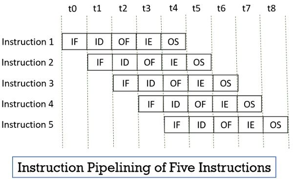 This pipeline has five stages: instruction fetch, instruction decode, operand fetch, instruction execute, operand store.
Credit: https://binaryterms.com/instruction-pipelining.html
This pipeline has five stages: instruction fetch, instruction decode, operand fetch, instruction execute, operand store.
Credit: https://binaryterms.com/instruction-pipelining.html
Superscalar architectures
The definition of "superscalar" has evolved somewhat over time. It is now used to describe processors that issue multiple instructions—often four or six—in a single clock cycle. Of course, a superscalar CPU must have multiple functional units to hand all these instructions to.
2.1.6 Processor-level parallelism
Instruction-level parallelism helps a little, but pipelining and superscalar operation rarely win more than a factor of five or ten. To get gains of 50, 100, or more, the only way is to design computers with multiple CPUs, so we will now take a look at how some of these are organized.
Data parallel computers
A substantial number of problems in computational domains such as the physical sciences, engineering, and computer graphics involve loops and arrays, or otherwise have a highly regular structure. Often the same calculations are performed repeatedly on many different sets of data. The regularity and structure of these programs makes them especially easy targets for speed-up through parallel execution. Two primary methods have been used to execute these highly regular programs quickly and efficiently: SIMD processors and vector processors.
-
A Single Instruction-stream Multiple Data-stream or SIMD processor consists of a large number of identical processors that perform the same sequence of instructions on different sets of data.
-
A vector processor appears to the programmer very much like a SIMD processor. Like a SIMD processor, it is very efficient at executing a sequence of operations on pairs of data elements. But unlike a SIMD processor, all of the operations are performed in a single, heavily pipelined functional unit.
Multiprocessors
Our first parallel system with multiple full-blown CPUs is the multiprocessor, a system with more than one CPU sharing a common memory, like a group of people in a room sharing a common blackboard. Since each CPU can read or write any part of memory, they must coordinate (in software) to avoid getting in each other’s way.
 Credit: https://zitoc.com/multiprocessor-system/
Multicomputers
Although multiprocessors with a modest number of processors (≤ 256) are relatively easy to build, large ones are surprisingly difficult to construct. The difficulty is in connecting so many the processors to the memory. To get around these problems, many designers have simply abandoned the idea of having a shared memory and just build systems consisting of large numbers of interconnected computers, each having its own private memory, but no common memory. These systems are called multicomputers. The CPUs in a multicomputer are said to be loosely coupled, to contrast them with the tightly coupled multiprocessor CPUs.
2.2 Primary memory
The memory is that part of the computer where programs and data are stored.
2.2.5 Cache memory
Historically, CPUs have always been faster than memories. What this imbalance means in practice is that after the CPU issues a memory request, it will not get the word it needs for many CPU cycles. The slower the memory, the more cycles the CPU will have to wait.
Actually, the problem is not technology, but economics. Engineers know how to build memories that are as fast as CPUs, but to run them at full speed, they have to be located on the CPU chip (because going over the bus to memory is very slow). What we would prefer is a large amount of fast memory at a low price. Interestingly enough, techniques are known for combining a small amount of fast memory with a large amount of slow memory to get the speed of the fast memory (almost) and the capacity of the large memory at a moderate price. The small, fast memory is called a cache.
The basic idea behind a cache is simple: the most heavily used memory words are kept in the cache. When the CPU needs a word, it first looks in the cache. Only if the word is not there does it go to main memory. Ifasubstantial fraction of the words are in the cache, the average access time can be greatly reduced.
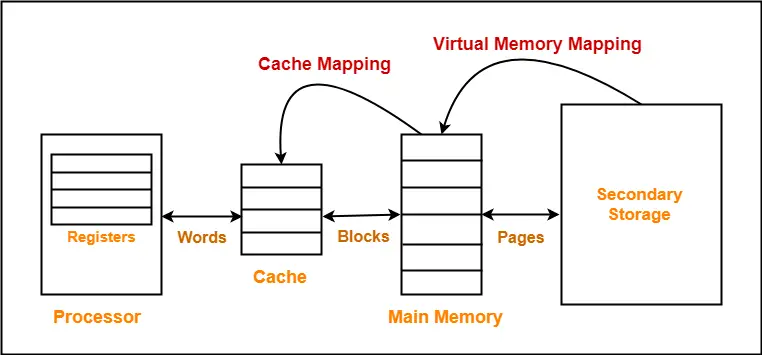 Illustration of cache memory, and virtual memory.
Credit: https://www.gatevidyalay.com/cache-mapping-cache-mapping-techniques/
Illustration of cache memory, and virtual memory.
Credit: https://www.gatevidyalay.com/cache-mapping-cache-mapping-techniques/
Locality principle
The locality principle is the observation that the memory references made in any short time interval tend to use only a small fraction of the total memory.
-
Temporal Locality: Programs tend to access the same data repeatedly over time. That is, if a program has used a variable recently, it’s likely to use that variable again soon.
-
Spatial Locality: Programs tend to access data that is nearby other, previously-accessed data. "Nearby" here refers to the data’s memory address. For example, if a program accesses data at addresses N and N+4, it’s likely to access N+8 soon.
The general idea is that when a word is referenced, it and some of its neighbors are brought from the large slow memory into the cache, so that the next time it is used, it can be accessed quickly.
Mean access time
Let be the cache access time, the main memory access time, and the hit ratio. We can calculate the mean access time as follows:
Cache design
- Cache size: the bigger the cache, the better it performs, but also the slower it is to access and the more it costs.
- Cache line size: Example: a 16-KB cache can be divided up into 1024 lines of 16 bytes, 2048 lines of 8 bytes, and other combinations.
- Organization of the cache: how does the cache keep track of which memory words are currently being held?
- Unified or split cache: should instructions and data use the same cache?
- Number of caches: It is common these days to have chips with a primary cache on chip, a secondary cache off chip but in the same package as the CPU chip, and a third cache still further away (L1, L2, L3).
2.3 Secondary memory
No matter how big the main memory is, it is generally way too small to hold all the data people want to store.
2.3.1 Memory hierarchies
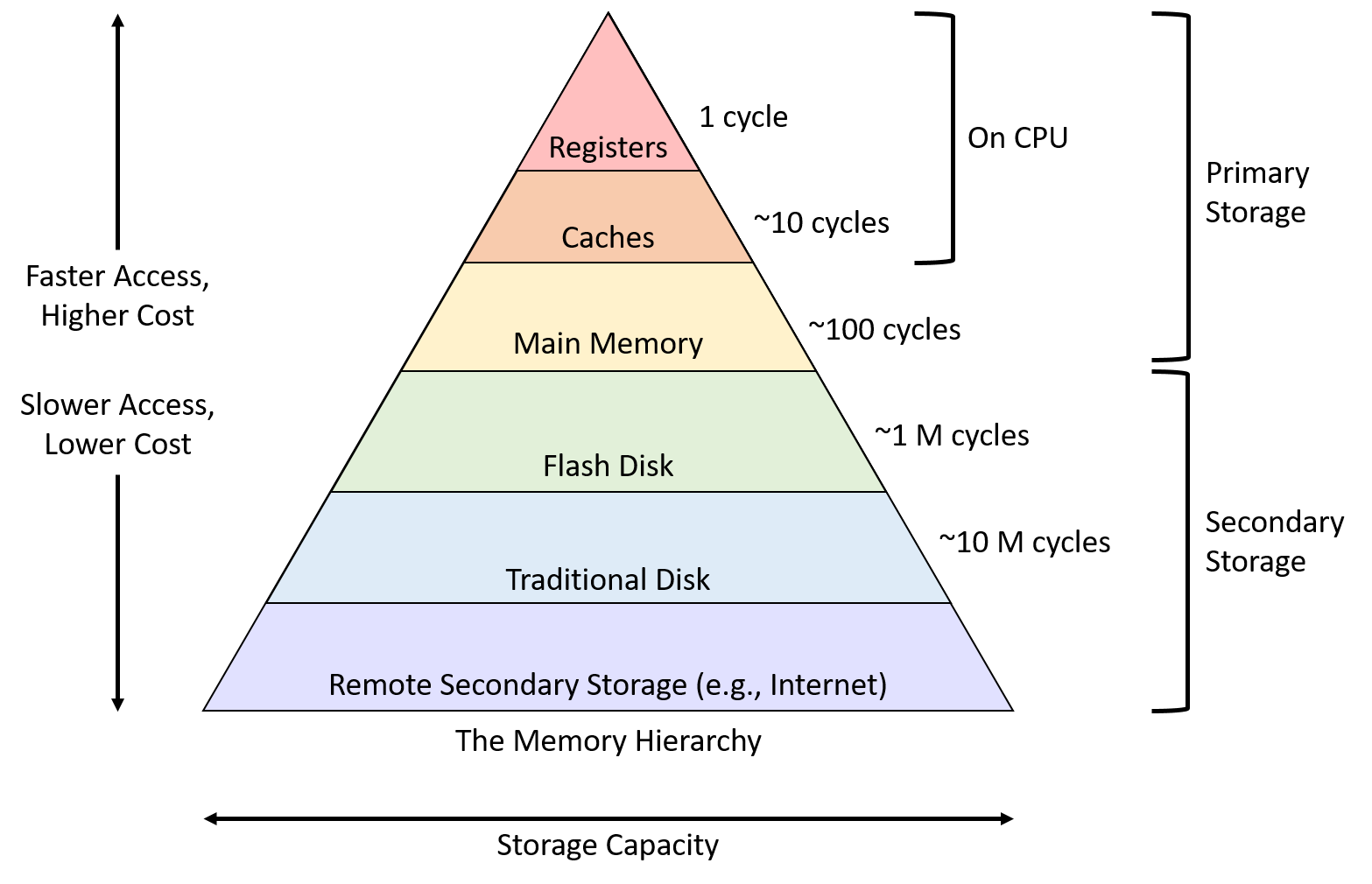 Credit: https://diveintosystems.org/book/C11-MemHierarchy/mem_hierarchy.html
2.4 Input and output (I/O)
As we mentioned at the start of this chapter, a computer system has three major components: the CPU, the memories (primary and secondary), and the I/O (Input/Output).
2.4.1 Buses
External devices exchange information with the CPU in the same way we generally exchange information in a computer, through buses.
Interrupt handler
A controller that reads or writes data to or from memory without CPU intervention is said to be performing Direct Memory Access (DMA). When the transfer is completed, the controller normally causes an interrupt, forcing the CPU to immediately suspend running its current program and start running a special procedure, called an interrupt handler, to check for errors, take any special action needed, and inform the operating system that the I/O is now finished. When the interrupt handler is finished, the CPU continues with the program that was suspended when the interrupt occurred.
Bus arbiter
What happens if the CPU and an I/O controller want to use the bus at the same time? The answer is that a chip called a bus arbiter decides who goes next. In general, I/O devices are given preference over the CPU, because disks and other moving devices cannot be stopped, and forcing them to wait would result in lost data. When no I/O is in progress, the CPU can have all the bus cycles for itself to reference memory.
Digital logic level
3.2 Basic digital logic circuits
3.2.2 Combinational circuits
Multiplexers
A multiplexer is a circuit with data inputs, one data output, and control inputs that select one of the data inputs.
Decoders
A decoder is a circuit that takes an -bit number as input and uses it to select (i.e., set to ) exactly one of the output lines.
3.2.3 Arithmetic circuits
Adders
Half adder
A half adder takes two 1-bit inputs and and outputs , the sum of the inputs, and , the carry bit. It is built from one AND-gate and one XOR-gate.
Full adder
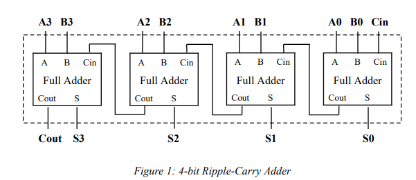
A full adder takes three 1-bit inputs , and , (carry in) and outputs , the sum of the inputs, and , the carry bit. It is built from two half adders.
Ripple carry adder
To build an adder for, say, two 16-bit words, one just replicates the full adder 16 times. The carry out of a bit is used as the carry into its left neighbor. The carry into the rightmost bit is wired to 0. This type of adder is called a ripple carry adder, because in the worst case, adding 1 to 111...111 (binary), the addition cannot complete until the carry has rippled all the way from the rightmost bit to the leftmost bit. Adders that do not have this delay, and hence are faster, also exist and are usually preferred.
 Credit: https://www.maxybyte.com/p/contents-1-introduction-1.html
3.3 Memory
3.3.2 Flip-flops
In many circuits it is necessary to sample the value on a certain line at a particular instant in time and store it. In this variant, called a flip-flop, the state transition occurs not when the clock is 1 but during the clock transition from 0 to 1 (rising edge) or from 1 to 0 (falling edge) instead. Thus, the length of the clock pulse is unimportant, as long as the transitions occur fast.
3.3.3 Registers
Flip-flops can be combined in groups to create registers, which hold data types larger than 1 bit in length.
3.3.5 Memory chips
A memory chip usually needs an address bus, data bus and a few control signals. CS (chip select) is used to select (enable) the chip.
3.3.6 RAMs and ROMs
SRAM vs DRAM
RAMs come in two varieties, static and dynamic. Static RAMs (SRAMs) are constructed internally using circuits similar to our basic D flip-flop. These memories have the property that their contents are retained as long as the power is kept on: seconds, minutes, hours, even days. Static RAMs are very fast. A typical access time is on the order of a nanosecond or less. For this reason, static RAMS are popular as cache memory. Dynamic RAMs (DRAMs), in contrast, do not use flip-flops. Instead, a dynamic RAM is an array of cells, each cell containing one transistor and a tiny capacitor. The capacitors can be charged or discharged, allowing 0s and 1s to be stored. Because the electric charge tends to leak out, each bit in a dynamic RAM must be refreshed (reloaded) every few milliseconds to prevent the data from leaking away. Because external logic must take care of the refreshing, dynamic RAMs require more complex interfacing than static ones, although in many applications this disadvantage is compensated for by their larger capacities. Since dynamic RAMs need only one transistor and one capacitor per bit (vs. six transistors per bit for the best static RAM), dynamic RAMs have a very high density (many bits per chip). For this reason, main memories are nearly always built out of dynamic RAMs. However, this large capacity has a price: dynamic RAMs are slow (tens of nanoseconds). Thus, the combination of a static RAM cache and a dynamic RAM main memory attempts to combine the good properties of each.
Nonvolatile memory chips (ROMs)
RAMs are not the only kind of memory chips. In many applications, such as toys, appliances, and cars, the program and some of the data must remain stored even when the power is turned off. Furthermore, once installed, neither the program nor the data are ever changed. These requirements have led to the development of ROMs (Read-Only Memories), which cannot be changed or erased, intentionally or otherwise. The data in a ROM are inserted during its manufacture, essentially by exposing a photosensitive material through a mask containing the desired bit pattern and then etching away the exposed (or unexposed) surface. The only way to change the program in a ROM is to replace the entire chip.
3.4 CPU chips and buses
3.4.2 Computer buses
A bus is a common electrical pathway between multiple devices. Buses can be categorized by their function. They can be used internal to the CPU to transport data to and from the ALU, or external to the CPU to connect it to memory or to I/O devices. Each type of bus has its own requirements and properties.
Bus protocol
In order to make it possible for boards designed by third parties to attach to the system bus, there must be well-defined rules about how the external bus works, which all devices attached to it must obey. These rules are called the bus protocol.
Some devices that attach to a bus are active and can initiate bus transfers, whereas others are passive and wait for requests. The active ones are called masters; the passive ones are called slaves. When the CPU orders a disk controller to read or write a block, the CPU is acting as a master and the disk controller is acting as a slave.
3.4.3 Bus width
The more address lines a bus has, the more memory the CPU can address directly. If a bus has address lines, then a CPU can use it to address different memory locations.
Multiplexed bus
Therefore the usual approach to improving performance is to add more data lines. As you might expect, however, this incremental growth does not lead to a clean design in the end. To get around the problem of very wide buses, sometimes designers opt for a multiplexed bus. In this design, instead of the address and data lines being separate, there are, say, 32 lines for address and data together. At the start of a bus operation, the lines are used for the address. Later on, they are used for data. For a write to memory, for example, this means that the address lines must be set up and propagated to the memory before the data can be put on the bus. Multiplexing the lines reduces bus width (and cost) but results in a slower system.
3.4.4 Bus clocking
Buses can be divided into two distinct categories depending on their clocking. A synchronous bus has a line driven by a crystal oscillator. The signal on this line consists of a square wave with a frequency generally between 5 and 133 MHz. All bus activities take an integral number of these cycles, called bus cycles. The other kind of bus, the asynchronous bus, does not have a master clock. Bus cycles can be of any length required and need not be the same between all pairs of devices.
3.4.5 Bus arbitration
"What happens if two or more devices all want to become bus master at the same time?" The answer is that some bus arbitration mechanism is needed to prevent chaos. Arbitration mechanisms can be centralized or decentralized. In centralized arbitration, a single bus arbiter determines who goes next. Decentralized arbitration can be implemented in several ways, but it usually involves that the devices must check if the bus is free to use before using it.
3.4.6 Bus operations
Block transfer
Often block transfers can be made more efficient than successive individual transfers. When a block read is started, the bus master tells the slave how many words are to be transferred, for example, by putting the word count on the data lines. Instead of just returning one word, the slave outputs one word during each cycle until the count has been exhausted.
Read-modify-write bus cycle
Allows any CPU to read a word from memory, inspect and modify it, and write it back to memory, all without releasing the bus. This type of cycle prevents competing CPUs from being able to use the bus and thus interfere with the first CPU’s operation.
Interrupts
When the CPU commands an I/O device to do something, it usually expects an interrupt when the work is done. The interrupt signaling requires the bus. Since multiple devices may want to cause an interrupt simultaneously, the same kind of arbitration problems are present here that we had with ordinary bus cycles. The usual solution is to assign priorities to devices and use a centralized arbiter to give priority to the most time-critical devices.
Microarchitecture level
4.2 An example ISA: IJVM
Low priority
- 4.2.1 Stacks
- 4.2.2 The IJVM memory model
- 4.2.3 The IJVM instruciton set
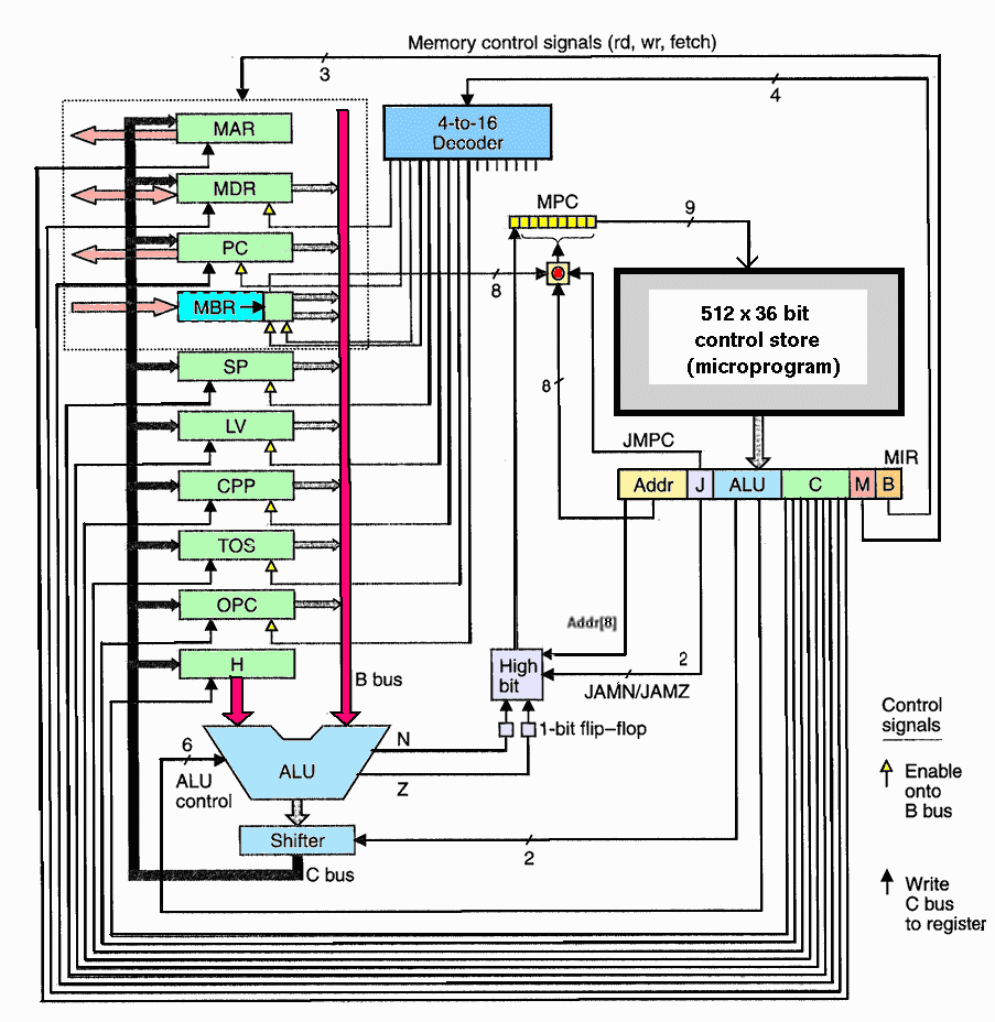 The IJVM microarchitecture.
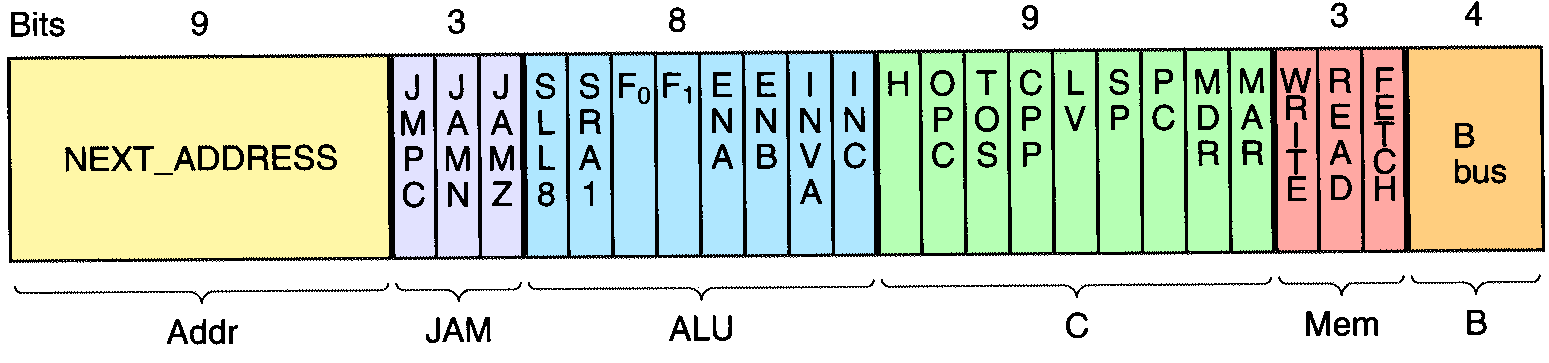 The IJVM microinstruction format.
Credit: https://users.cs.fiu.edu/~prabakar/cda4101/Common/notes/lecture17.html
The IJVM microinstruction format.
Credit: https://users.cs.fiu.edu/~prabakar/cda4101/Common/notes/lecture17.html
4.3 An example implementation
Low priority
- 4.3.1 Microinstructions and notation
- 4.3.2 Implementation of IJVM using the mic-1
4.4 Design of the microarchitecture level
4.4.1 Speed versus cost
Speed can be measured in a variety of ways, but given a circuit technology and an ISA, there are three basic approaches for increasing the speed of execution:
- Reduce the number of clock cycles needed to execute an instruction.
- Simplify the organization so that the clock cycle can be shorter.
- Overlap the execution of instructions
The following (4.4.2 - 4.4.5) might be useful, but have not been prioritized. Read the book for details.
- 4.4.2 Reducing the execution path length
- 4.4.3 A design with prefetching: the mic-2
- 4.4.4 A pipelined design: the mic-3
- 4.4.5 A seven-stage pipeline: the mic-4
4.5 Improving performance
4.5.1 Cache memory
See 2.2.5 Cache memory for an introduction to caches.
All caches use the following model. Main memory is divided up into fixed size blocks called cache lines. A cache line typically consists of 4 to 64 consecutive bytes. Lines are numbered consecutively starting at 0, so with a 32-byte line size, line 0 is bytes 0 to 31, line 1 is bytes 32 to 63, and so on. At any instant, some lines are in the cache. When memory is referenced, the cache controller circuit checks to see if the word referenced is currently in the cache. If so, the value there can be used, saving a trip to main memory. If the word is not there, some line entry is removed from the cache and the line needed is fetched from memory or more distant cache to replace it.
Direct-mapped caches
The simplest cache is known as a direct-mapped cache. Each cache entry consists of three parts:
- The
Validbit indicates whether there is any valid data in this entry or not. When the system is booted (started), all entries are marked as invalid. - The
Tagfield consists of a unique, 16-bit value identifying the corresponding line of memory from which the data came. - The
Datafield contains a copy of the data in memory. This field holds one cache line of 32 bytes.
In a direct-mapped cache, a given memory word can be stored in exactly one place within the cache. Given a memory address, there is only one place to look for it in the cache. If it is not there, then it is not in the cache.
Set-associative caches
As mentioned above, many different lines in memory compete for the same cache slots. If a program heavily uses words at addresses 0 and at 65,536, there will be constant conflicts, with each reference potentially evicting the other one from the cache. A solution is to allow two or more lines in each cache entry. A cache with n possible entries for each address is called an n-way set-associative cache.
When a new entry is to be brought into the cache, which of the present items should be discarded? The optimal decision, of course, requires a peek into the future, but a pretty good algorithm for most purposes is LRU (Least Recently Used). This algorithm keeps an ordering of each set of locations that could be accessed from a given memory location. Whenever any of the present lines are accessed, it updates the list, marking that entry the most recently accessed. When it comes time to replace an entry, the one at the end of the list—the least recently accessed—is the one discarded.
4.5.2 Branch prediction
With good branch prediction, we often don't need to wait for the condition instruction to complete the pipeline before stepping to the next instruction. If the prediction is wrong however, we must backtrack to the branch and take the other route. This may involve a flush of the pipeline.
With dynamic branch prediction, branches are predicted at run-time. If a branch has been chosed previously, it will be chosen again. A history table of the branches must be stored.
With static branch prediction, branches are predicted at compile-time.
8.1 On-chip parallelism
8.1.1 Instruction-level parallelism (ILA)
Multiple-issue CPUs come in two varieties: superscalar processors and VLIW (Very Long Instruction Word) processors.
In effect, VLIW shifts the burden of determining which instructions can be issued together from run time to compile time. Not only does this choice make the hardware simpler and faster, but since an optimizing compiler can run for a long time if need be, better bundles can be assembled than what the hardware could do at run time.
8.1.2 On-chip multithreading
All modern, pipelined CPUs have an inherent problem: when a memory reference misses the level1and level2caches, there is a long wait until the requested word (and its associated cache line) are loaded into the cache, so the pipeline stalls. One approach to dealing with this situation, called on-chip multithreading, allows the CPU to manage multiple threads of control at the same time in an attempt to mask these stalls. In short, if thread 1 is blocked, the CPU still has a chance of running thread 2 in order to keep the hardware fully occupied.
The three main ways of doing on-chip multithreading are:
- Fine-grained multithreading
- Coarse-grained multithreading
- Simultaneous multithreading
Instruction set architecture level (ISA)
5.1 Overview of the ISA level
5.1.1 Properties of the ISA level
In principle, the ISA level is defined by how the machine appears to a machine-language programmer. Since no (sane) person does much programming in machine language any more, let us redefine this to say that ISA-level code is what a compiler outputs. To produce ISA-level code, the compiler writer has to know what the memory model is, what registers there are, what data types and instructions are available, and so on. The collection of all this information is what defines the ISA level.
5.1.2 Memory models
All computers divide memory up into cells that have consecutive addresses. Bytes are generally grouped into 4-byte (32-bit) or 8-byte (64-bit) words with instructions available for manipulating entire words.
Most machines have a single linear address space at the ISA level, extending from address 0 up to some maximum, often bytes or bytes. However, a few machines have separate address spaces for instructions and data (Hardvard-architecture), so that an instruction fetch at address 8 goes to a different address space than a data fetch at address 8. This scheme is more complex than having a single address space, but it has two advantages. First, it becomes possible to have bytes of program and an additional bytes of data while using only 32-bit addresses. Second, because all writes automatically go to data space, it becomes impossible for a program to accidentally overwrite itself, thus eliminating one source of program bugs.
5.1.3 Registers
All computers have some registers visible at the ISA level. They are there to control execution of the program, hold temporary results, and serve other purposes.
ISA-level registers can be roughly divided into two categories: special-purpose registers and general-purpose registers The special-purpose registers include things like the program counter and stack pointer, as well as other registers with a specific function. In contrast, the general-purpose registers are there to hold key local variables and intermediate results of calculations. Their main function is to provide rapid access to heavily used data (basically, avoiding memory accesses). RISC machines, with their fast CPUs and (relatively) slow memories, usually have at least 32 general-purpose registers, and the trend in new CPU designs is to have even more.
One control register that is something of a kernel/user hybrid is the flags register or PSW (Program Status Word). This register holds various miscellaneous bits that are needed by the CPU. The most important bits are the condition codes. These bits are set on every ALU cycle and reflect the status of the result of the most recent operation. Typical condition code bits include
- N — Set when the result was Negative.
- Z — Set when the result was Zero.
- V — Set when the result caused an oVerflow.
- C — Set when the result caused a Carry out of the leftmost bit.
- A — Set when there was a carry out of bit 3 (Auxiliary carry—see below).
- P — Set when the result had even Parity.
The condition codes are important because the comparison and conditional branch instructions use them. For example, the CMP instruction typically subtracts two operands and sets the condition codes based on the difference. If the operands are equal, then the difference will be zero and the Z condition code bit in the PSW register will be set. A subsequent BEQ instruction tests the Z bit and branches if it is set.
5.3 Instruction formats
An instruction consists of an opcode, usually along with some additional information such as where operands come from and where results go to.
5.3.1 Design criteria for instruction formats
- Short instructions are better than long ones.
- Sufficient room in the instruction format to express all the operations desired.
- The number of bits in an address field.
5.3.1 Expanding opcodes
The idea of expanding opcodes demonstrates a trade-off between the space for opcodes and space for other information.
5.4 Addressing
Most instructions have operands, so some way is needed to specify where they are. This subject, which we will now discuss, is called addressing.
5.4.2 Immidiate addressing
The simplest way for an instruction to specify an operand is for the address part of the instruction actually to contain the operand itself rather than an address or other information describing where the operand is. Such an operand is called an immediate operand because it is automatically fetched from memory at the same time the instruction itself is fetched; hence it is immediately available for use.
Example: MOV R0,
5.4.3 Direct addressing
A method for specifying an operand in memory is just to give its full address. This mode is called direct addressing. Like immediate addressing, direct addressing is restricted in its use: the instruction will always access exactly the same memory location. So while the value can change, the location cannot.
Example: LOAD R0, #0xFFFF 1000
5.4.4 Register addressing
Register addressing is conceptually the same as direct addressing but specifies a register instead of a memory location. Because registers are so important (due to fast access and short addresses) this addressing mode is the most common one on most computers. This addressing mode is known simply as register mode. In load/store architectures, nearly all instructions use this addressing mode exclusively.
Example: MOV R0, R1
5.4.5 Register indirect addressing
In this mode, the operand being specified comes from memory or goes to memory, but its address is not hardwired into the instruction, as in direct addressing. Instead, the address is contained in a register. An address used in this manner is called a pointer. A big advantage of register indirect addressing is that it can reference memory without paying the price of having a full memory address in the instruction.
Example: LOAD R0, (R1)
5.4.6 Indexed addressing
Addressing memory by giving a register (explicit or implicit) plus a constant offset is called indexed addressing.
Example: LOAD R0, #100(R1)
5.4.7 Based-Indexed Addressing
Some machines have an addressing mode in which the memory address is computed by adding up two registers plus an (optional) offset. Sometimes this mode is called based-indexed addressing.
Example: LOAD R0, (R1 + R2)
5.5 Instruction types
5.5.1 Data movement instructions
Copying data from one place to another is the most fundamental of all operations. Since there are two possible sources for a data item (memory or register), and there are two possible destinations for a data item (memory or register), four different kinds of copying are possible. Some computers have four instructions for the four cases. Others have one instruction for all four cases. Still others use LOAD to go from memory to a register, STORE to go from a register to memory, MOVE to go from one register to another register, and no instruction for a memory-to-memory copy.
5.5.2 Dyadic operations
Dyadic operations combine two operands to produce a result. All ISAs have instructions to perform addition and subtraction on integers. Another group of dyadic operations includes the Boolean instructions.
5.5.3 Monadic operations
Monadic operations have one operand and produce one result. Instructions to shift or rotate the contents of a word or byte are quite useful and are often provided in several variations. Shifts are operations in which the bits are moved to the left or right, with bits shifted off the end of the word being lost.
5.5.4 Comparisons and conditional branches
See last part of 5.1.3 Registers
5.5.5 Procedure call instructions
A procedure is a group of instructions that performs some task and that can be invoked (called) from several places in the program. The term subroutine is often used instead of procedure, especially when referring to assembly-language programs. In C, procedures are called functions. When the procedure has finished its task, it must return to the statement after the call. Therefore, the return address must be transmitted to the procedure or saved somewhere so that it can be located when it is time to return.
5.5.6 Loop control
The need to execute a group of instructions a fixed number of times occurs frequently and thus some machines have instructions to facilitate doing this. All the schemes involve a counter that is increased or decreased by some constant once each time through the loop. The counter is also tested once each time through the loop. If a certain condition holds, the loop is terminated.
5.5.7 Input/output
No other group of instructions exhibits as much variety from machine to machine as the I/O instructions. Three different I/O schemes are in current use in personal computers. These are
- Programmed I/O with busy waiting.
- Interrupt-driven I/O.
- DMA I/O.
Virtual memory
6.1 Virtual memory
Virtual memory is a storage allocation scheme in which secondary memory can be addressed as though it were part of the main memory.
See memory caching for an illustraion.
6.1.1 Paging
The technique for automatic overlaying is called paging and the chunks of program read in from disk are called pages. A memory map or page table specifies for each virtual address what the corresponding physical address is.
Programs are written just as though there were enough main memory for the whole virtual address space, even though that is not the case. Programs may load from, or store into, any word in the virtual address space, or branch to any instruction located anywhere within the virtual address space, without regard to the fact that there really is not enough physical memory. In fact, the programmer can write programs without even being aware that virtual memory exists. The computer just looks as if it has a big memory.
6.1.2 Implementation of paging
Every computer with virtual memory has a device for doing the virtual-to-physical mapping. This device is called the MMU (Memory Management Unit).
6.1.3 Demand paging and the working-set model
When a reference is made to an address on a page not present in main memory, it is called a page fault. After a page fault has occurred, the operating system must read in the required page from the disk, enter its new physical memory location in the page table, and then repeat the instruction that caused the fault. (Similar to a cache miss).
In demand paging, a page is brought into memory only when a request for it occurs, not in advance.
6.1.4 Page-replacement policy
Ideally, the set of pages that a program is actively and heavily using, called the working set, can be kept in memory to reduce page faults. However, programmers rarely know which pages are in the working set, so the operating system must discover this set dynamically. When a program references a page that is not in main memory, the needed page must be fetched from the disk. To make room for it, however, some other page will generally have to be sent back to the disk. Thus an algorithm that decides which page to remove is needed. As with set associative caches, we may use the Least Recently Used-algorithm. Another page-replacement algorithm is FIFO (First-In First-Out).
6.1.5 Page size and fragmentation
The "last page" of a program is often not completely filled, and will waste space when it is in memory. This is called internal fragmentation. The are multiple positives and negatives to both large and small sizes.
| Small pages | Large pages |
|---|---|
| Less waste 👍 | More waste 👎 |
| Large page table 👎 | Small page table 👍 |
| Inefficient use of disk bandwidth 👎 | Efficient use of disk bandwidth 👍 |
| All things considered, the trend is toward larger page sizes. In practice, 4 KB is the minimum these days. |